Before we start it, I must declare that most contents that I summarized in this article can be derived from this online paper: Clock Domain Crossing (CDC) Design & Verification Techniques Using SystemVerilog. If you want to dig into some details that I mentioned in this article, you can read that paper as reference. CDC is a common but also tricky problem. It is also usually the first problem that you are very likely to encounter with when you are struggling to put your first fully-functional-verified design onto a FPGA development board. Before we go any further, I want you to remember 4 golden rules that you must follow to avoid CDC troubles.
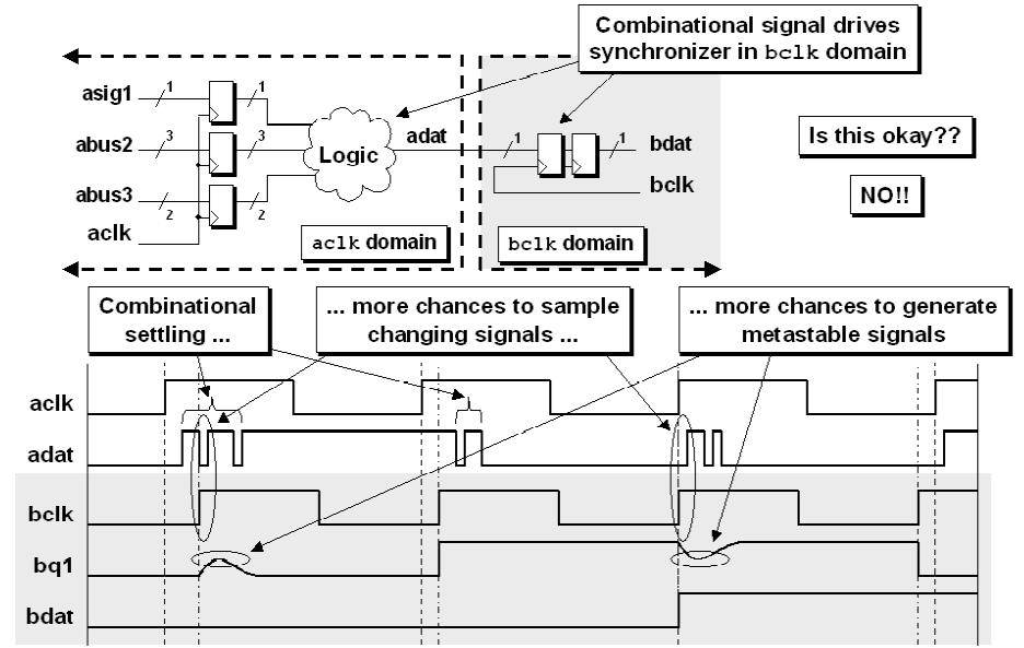
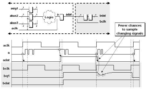
- Rule 1, Register The Signals Before Crossing!!!
Reason: The register at the edge will filter out the combinational settling to deliver clean data to cross the CDC boundary.
- Rule 2, Change One Signal Only Each Time!!!
Reason: General synchronizer could not handle the misalignment between multiple signals
- Rule 3, Hold The Signal For Over 3 Clock Edges In Target Domain!!!
Reason: This is to ensure that the sampling process would have been done for sure.
- Rule 4, Use Level Instead Of Pulse To Cross Clock Domains!!!
Reason: It is really hard to control the width of a pulse in the target domain.
I. What Is CDC Issue
SOME DEFINITIONS
- FAST Versus SLOW
We say the data changing is slow when it lasts more than 3 clock edges in the receiving clock domain
Likewise, we say it is fast when it changes within 1.5 cycles in the target domain.
- LEVEL Versus PULSE
There is never real level or pulse in a system, if a logic never toggle, it deliver no message at all, the question is, a pulse with how long in length would be acceptable when it takes crossing?
- SETUP / HOLD TIME & METASTABILITY
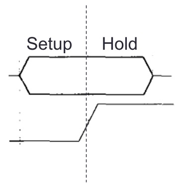
The time window during which data are required to stay stable, setup time refers to the period before clock sampling, while hold time refers to the period after it.

If the clock edge samples a data while it's changing, the sampled data are not assumed as either stable 0 or 1 state. Metastability can never be eliminated, normally we just isolate them in between of flip flops so that it will not go further beyond to mess up subsequent logic states.
For more information about setup time & hold time, please refer to this article: Why Do Setup Time And Hold Time Matter.
II. Different Synchronisers
"A synchronizer is a device that samples an asynchronous signal and outputs a version of the signal that has transitions synchronized to a local or sample clock."
Dally & Poulton
For most synchronization applications, the two flip-flop synchronizer is sufficient to remove all likely metastability.
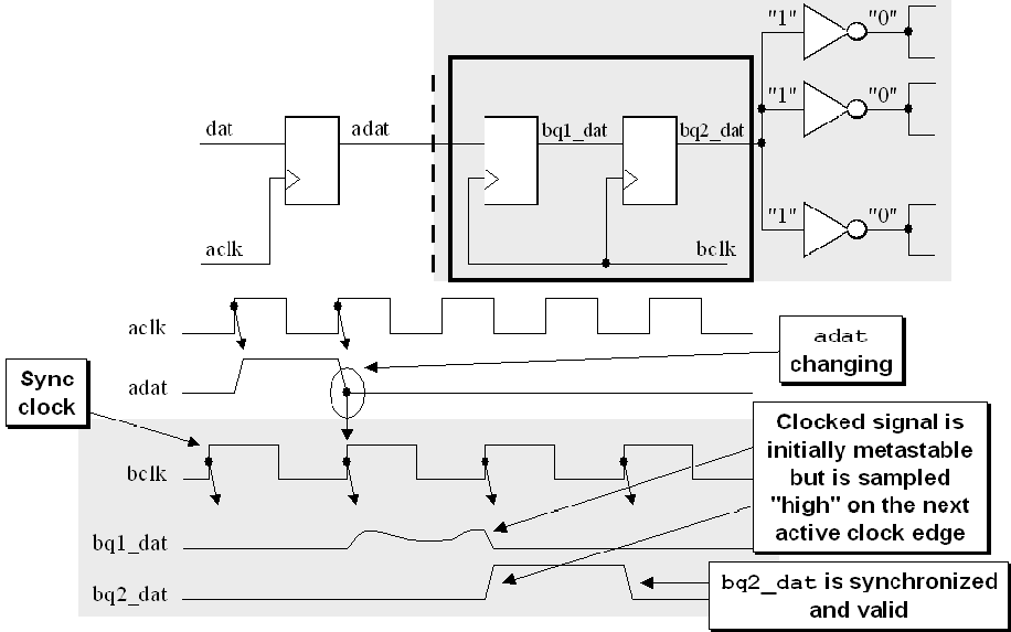
Two Flip-flop Synchronizer
The first flip-flop samples the asynchronous signal level into the new clock domain, and waits for a full clock cycle in the new clock domain to let any metastability to get settled. Then it’s sampled by the same clock into a second flip-flop with the intended goal that it’s ready for distribution within the new domain.

Three Flip-flop Synchronizer
For design with higher speed, two-flop synchronizer is too short so that a third flop is added to increase MTBF.

Synchroniser Is Not Omiponent
NO IF YOU IDIOTS FAILED TO REGISTER THE DATA BEFORE SEND!!!


This is where our Rule 1 come from, please always remember to register you signal before sending it to go across clock domains.

 中文
中文
对于多位位宽的跨时钟域传输,是不是只有用异步FIFO,RAM等缓冲区了?
其实只要遵守我提到的4条黄金定律,什么样的跨时钟域传输办法都可以开发出来啊,只要你脑洞够大。比如说,只要符合每次跨时钟域只改变一根信号线,那多比特位宽可以只改变一根信号线吗?你想想格雷码是不是可以做到?如果不是格雷码怎么办?可以用单比特的握手信号REQ延迟一拍同步到对面时钟域通过对面时钟同步后再传回产生ACK信号保证足够长的数据准备时间也可以保证数据稳定哦。其实思路有很多很多,但是本文一开始提到的4条黄金定律是铁律,只要满足的话,用什么办法都可以达到目的,只有效率的区别。本文内容来自我写的一份培训PPT,因为是全英文的,翻译传图比较花时间,所以一时还没贴完整。